Bron
Het verhaal
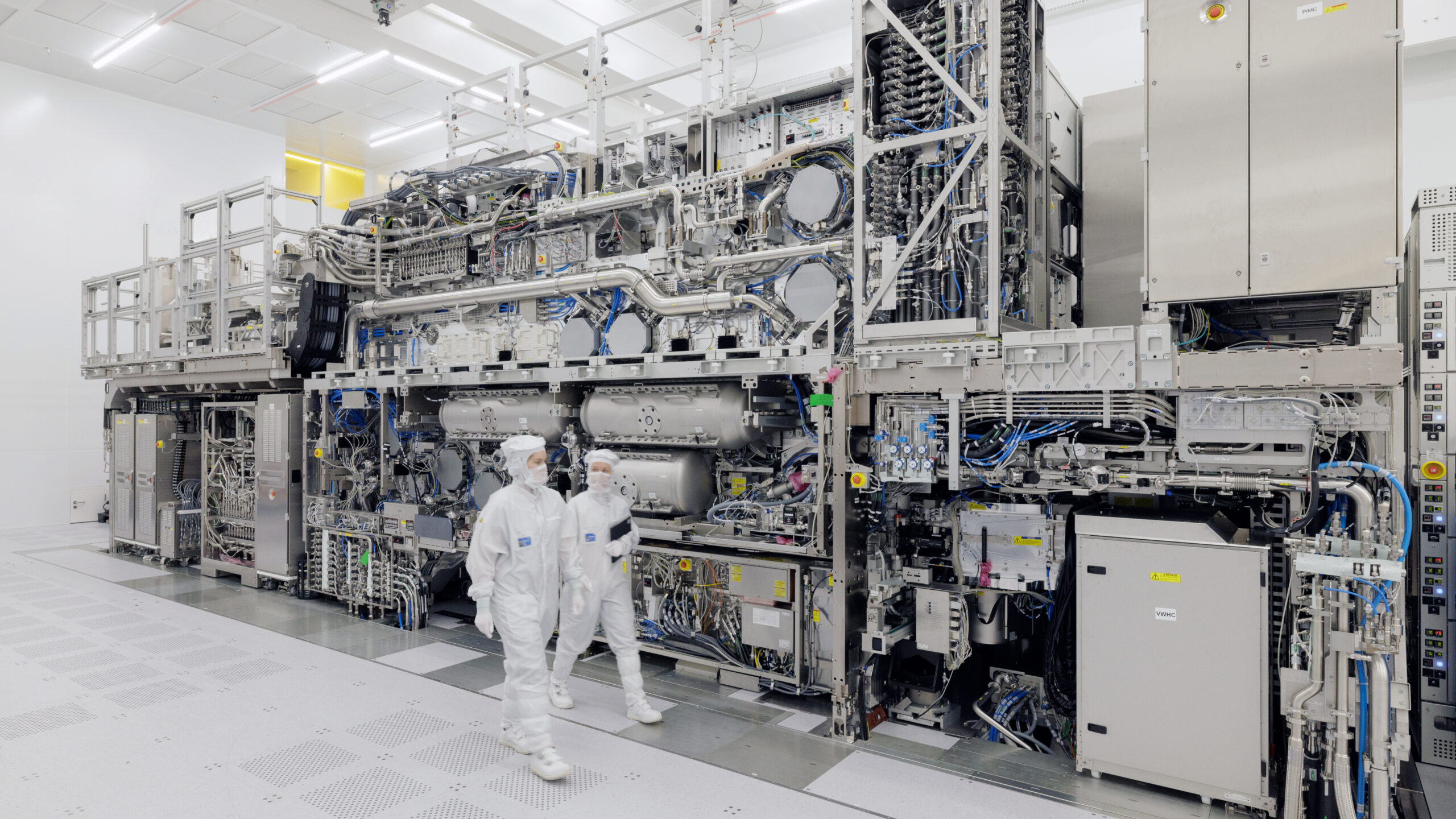
On 8 Sep 2026 Ars Technica reported that Samsung and TSMC are embracing ASML’s high-NA EUV lithography machines, which cost on the order of $400 million per tool. Samsung plans high-NA for memory roughly by 2028; TSMC is aiming high-NA at leading-edge logic around 2030. Alongside that adoption, Samsung, TSMC, and Intel agreed to shift photomasks from today’s 6-inch format to 12-inch masks — a change Ars ties to roughly 40% productivity gains in the mask/stepper workflow. The combo matters for AI chip capacity: more advanced nodes and higher mask throughput feed GPU/accelerator supply.